Nanogallery
Atomic Force Microscopy (AFM)
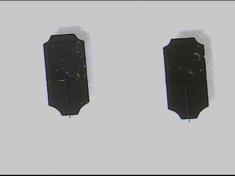
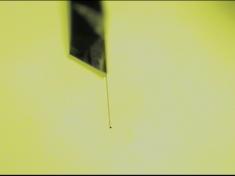
Top and side views of AFM cantilevers and tips mounted on a rectangular substrate, viewed at 45X magnification.
_512x384.jpg)
The cantilever and tip extend over a window in the AFM scanner to allow optical access.
AFM Images
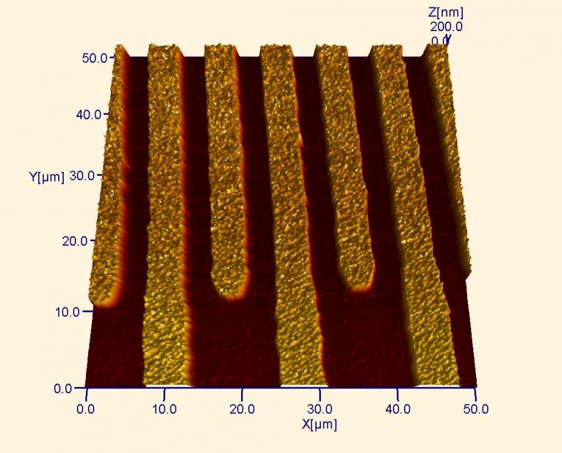
AFM micrograph of an interdigitated electrode array composed of 175 nm of Ti that was vapor deposited (after a photolithograph patterning step) onto a Si wafer. AFM allows highly accurate determination of the height of such a deposit (as seen in the cross-section below).
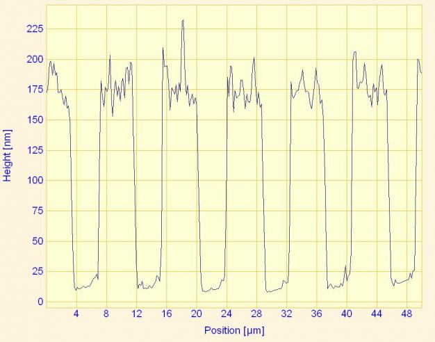
This is a cross-section of the electrode array from a previous image. It is the result of one horizontal scan of the AFM cantilever across the surface. This graph allows height information to be easily obtained.
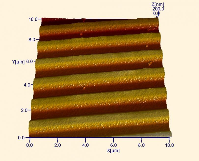
AFM image of a CD before any data is written. The raised ridges are used as “tracks” on which a laser writes data during the “burning” process.
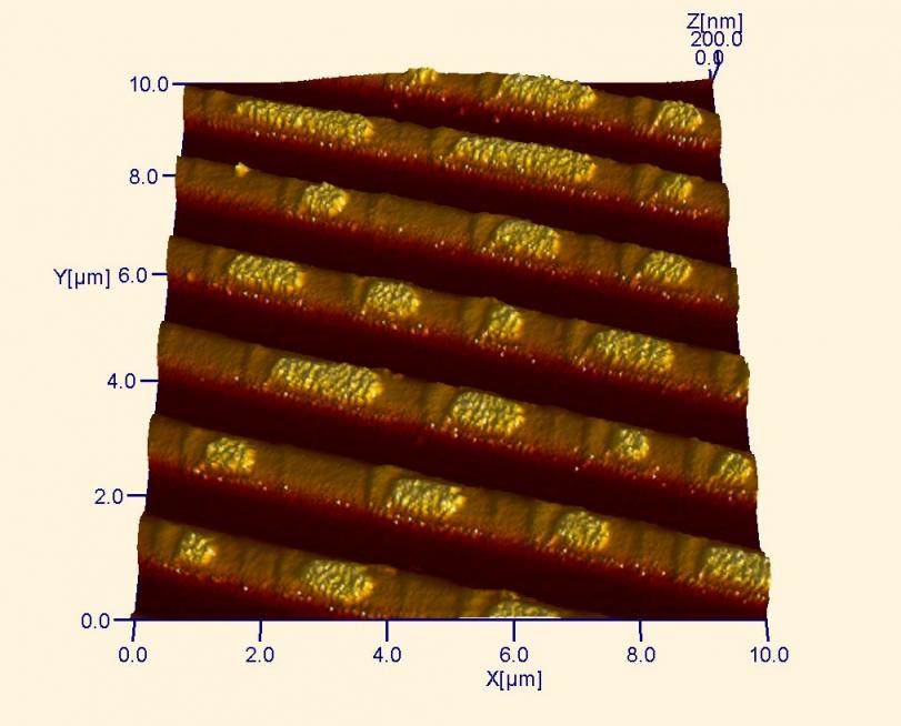
AFM image of a CD after data is written. Notice the raised spots on the tracks of the disk. These spots store the bits of information that are used to transfer information. AFM is often used to verify the quality of stamps used for making commercial CDs.
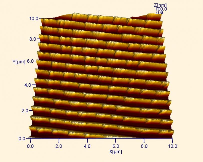
AFM image of a DVD after data is written. In this image, it is evident that the storage capacity of a DVD is much greater than the CD above, as the rows of “tracks” are much closer together.
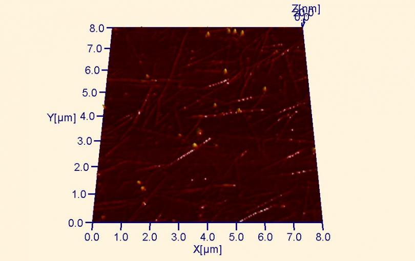
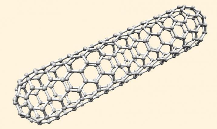
Single-walled carbon nanotube (SWNT) network composed of SWNTs deposited on a silicon wafer. Such networks are transparent, flexible and highly conductive over large areas, making them highly desirable electronic materials. SWNTs are nanometer-scale tubes made of graphite, the form of carbon found in pencils (below).
Scanning Tunneling Microscopy (STM)
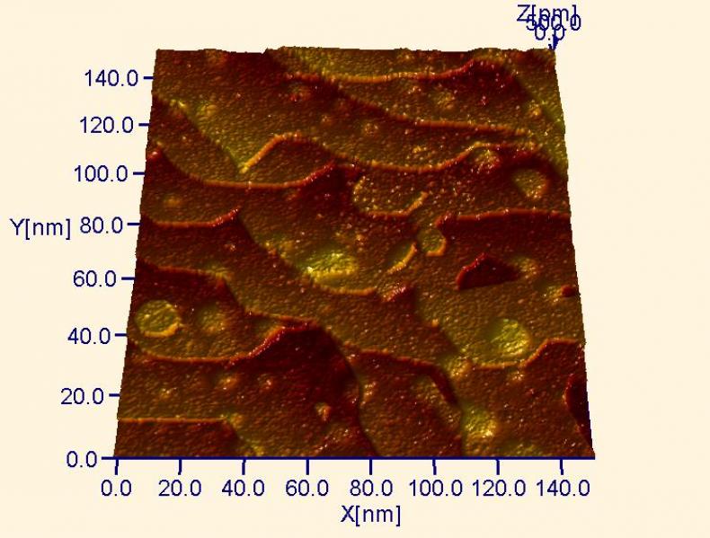
Large-scale ultra-high vacuum STM micrograph of a ruthenium (Ru) single crystal surface. The small Ru islands are a result of the preparation routine used to obtain a clean surface. Ion sputtering (like sandblasting with ions) was used to clean the surface. Ru is such a refractory metal that these small islands don’t coalesce with step edges even when the metal is heated to 1000º C, as with other metals (compare with gold below).
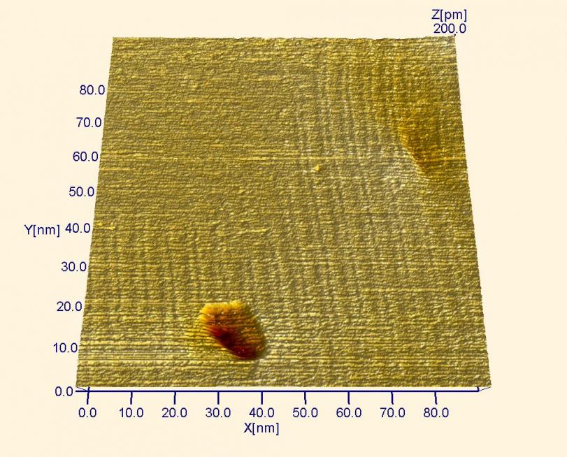
The “soliton” walls (pairs of parallel lines) of the gold reconstruction are visible in this image. This reconstruction forms spontaneously on a clean gold surface in air, liquid and vacuum. These soliton walls are only 0.2 nanometers (or 200 picometers) high, yet STM can image them easily! Two pits, surface defects, are also visible.
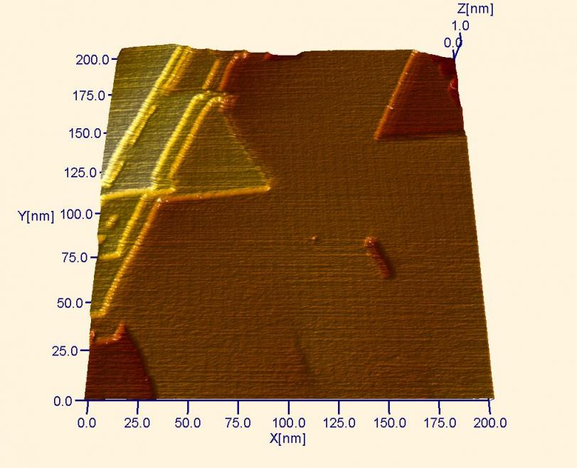
Large-scale STM image of the surface of a “gold-on-glass” sample. This was formed by vapor depositing gold onto a glass slide using a process called thermal evaporation. Each step seen above is a little less than one atomic layer higher than the next lower (darker) step. On the flat planes, the soliton walls of the gold reconstruction are visible even in this large scale image.
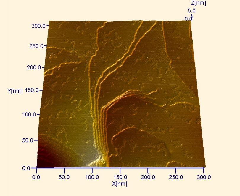
Large-scale STM image of the surface of a gold singe crystal. The gold reconstruction observed in previous images has been lifted by immersing this crystal in an electrolyte to prepare for an electrochemical experiement. The extra atoms that formed the soliton walls now aggregate into small islands on the surface.
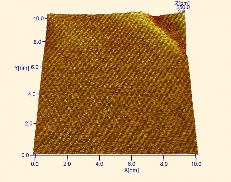
Gold (Au) atoms. Notice how the Au atoms appear lower than the HOPG atoms two images below. This is because Au is a true metal and each atom is surrounded by a sea of delocalized electrons. This property makes it more difficult to image the Au atoms, as they appear to have a low height.
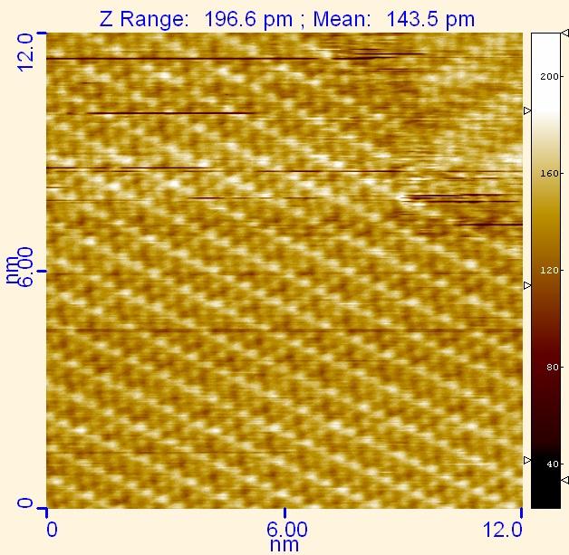
This image was obtained during the electrodeposition of tellurium on gold. At negative electrochemical potentials, tellurium atoms crowd onto the surface to form this pattern.
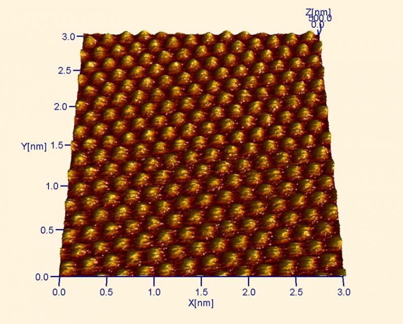
Atomic resolution image of highly oriented pyrolytic graphite (HOPG). Graphite is the same material in pencils, but it also conducts electricity very well. This is also the same form of C in carbon nanotubes. In this image, every other C atom is imaged.
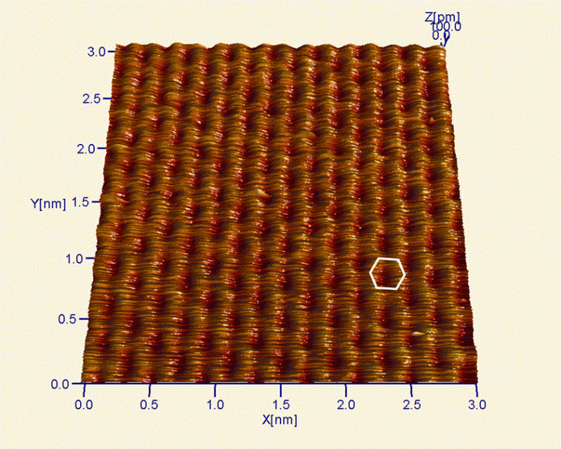
Every atom in HOPG is imaged when the STM tip is brought closer to the surface and the true hexagonal nature of the graphite is observed.

