Scanning Tunneling Microscopy (STM)
Scanning tunneling microscopy (STM) is a technique that can yield information about the geometry and density of electronic states and for atoms on the surface of samples that conduct electricity. STM is widely used in industrial as well as academic research because it can provide a real-space, real-time, atomic level view of conducting surfaces. STM works because a current can be made to flow between a conducting surface and a sharp metal tip when they are brought very close together. This is accomplished by applying a voltage between the sample and the tip. The tip, which ideally has just one atom at its apex, is then lowered toward the surface. As the tip comes to within a few nanometers (1 nanometer, nm = 1 billionth of a meter) of the surface, a finite current begins to flow as electrons bridge the gap between the tip and the sample. The tip is usually composed of tungsten (W), or an alloy of platinum and iridium (Pt/Ir).
As with AFM, the tip is mounted on a piezo-electric surface (see figure above). When a voltage is applied to a piezo-electric material, it produces a mechanical pressure that is directly proportional to the magnitude of the voltage. This gives the user very precise control over the movement of the tip. Because there is an exponential dependence of the tunnel current on the distance of the tip from the surface, very small fluctuations in the tunneling current can be detected and mapped. Therefore, the tip can be raster-scanned over a small area to create a contour of the electronic states present on the surface. The tip moves over a larger area in the x direction, then a small area in the y direction to create a square of a size determined by the microscope operator. A computer then transforms this electronic contour into an image of the surface morphology and/or local electronic structure.
There are two modes for STM. In height mode, or constant current mode, the sample-tip distance is kept constant. This is accomplished by means of a voltage applied to the piezo-electric material on which the tip is mounted. The tip is moved up or down (positive or negative on the z-axis) as it is raster-scanned across the surface, with the feedback loop keeping the measured current constant. The displacement of the tip on the z-axis is charted as a function of the x and y position. The feedback loop is used to control how fast the tip responds to changes in the measured current. This feedback loop can be adjusted to reduce noise and improve image quality.
In current mode, or constant height mode, the tip does not vary from its original position on the z-axis. The modulation in the current is plotted as a function of the tip’s position to provide the image of the surface. The height stays pretty much the same. There is very little feedback. Therefore, very high scan rates can be used. However, the tip will crash into any high area on the surface, so current mode is impractical for all but the flattest of substrates.
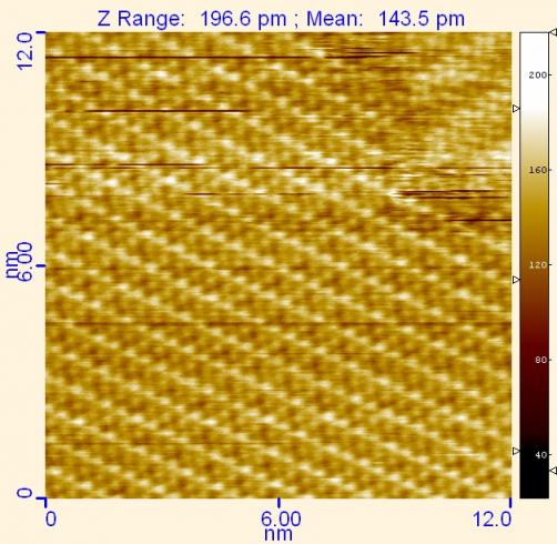
Click on the image below for a demonstration of the level of topographic information available with STM.


